The current version can be found here. This module consists of several parts, a pulse divider with integer divisions between 2 and 8, and several logic elements. The divider is used to generate interrelated pulses for use in creating poly-rhythms, and unusual sequences. It can also be run at audio frequencies as a sub-oscillator/sub harmonic generator. The output pulse from each division is one clock cycle in length, and the relationship between pulses is fixed. Specifically, the /4 output will correspond to every second pulse from the /2 output. Likewise, the /8 will correspond to every second pulse from the /4 output, and the /6 will correspond to every second pulse from the /3 output. Needless to say, the /2 and /3 groups are not related to each other, or to the /5 or /7 outputs. All however share a common external reset, so they can be synchronized. All outputs go high on reset. As well as the pulse divider, there are also four boolean logic elements. Two are basic inverters. If you apply a LOW (e.g. a gate output in its OFF state) they will give a HIGH (gate ON) output, and vice versa. The OR gate has two inputs, and gives a HIGH whenever one or both inputs are HIGH. The AND gate has two inputs, and gives a HIGH only when both inputs are HIGH. Both of these have built in LED monitors. Unlike the Analog Logic module, these are strictly for processing gate, trigger and clock signals. Some ideas on how to use this module: Feed a clock signal into the input of the pulse divider. The divided signal is available simultaneously for each output. If running at audio frequencies, feed some of these to a mixer or other signal processing device. If running at low speed, try driving two different sequencers at the same time from different divisions. Try feeding the /8 output into the reset - this will force all to synchronize to a /7 count, with the lesser divisions becoming "syncopated". The AND gate could be used to control a clock signal. If the second input is LOW, no clock signal passes. If the second input is high, the signal passes unimpeded. Of course, there are a lot more things that can be done with the logic gates. For example, the /6 and /7 outputs could be ANDed together, and that would give a pulse every 6 x 7 (42) clock pulses (i.e. 1 pulse immediately the pulse divider is reset, and the second 42 pulses after that etc.). A little on how it works:
Click here for the schematics:
The clock and reset signals are processed by the LM358 (or TL072). The reset is sensitive to rising edges only, meaning that a continuous gate signal would reset the dividers, then allow the module to continue counting. The Reset button on the other hand is wired so that holding it in will stop all counting, and hold all outputs high for as long as the button is held. Following the input processor are four 4017 decade counters wired to give the various divisions. Where possible, sub-divisions have been taken from the same chip, with the various pulses being ORed together by diodes. Each output is buffered by an emitter follower. Many small signal or switching transistors can be used here without affecting the performance. The boolean logic are simple discrete R/DTL designs. When either input of the OR gate receives a voltage high enough, the first transistor is switched on, pulling the base of the second transistor low, and thus turning it on as well. This results in the output being pulled up to the voltage governed by the resistor divider. In the case of the AND gate, both input transistors must be turned on before the output transistor can be turned on, as the input transistors are in series with each other. The inverters are basically just the same as the first stage of the OR gate, with the exception of there being only one input.
Construction

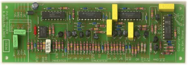
The component overlay. Click here for an enlarged printable version. Note: On the first run of the PCBs, the 820R and 680R in the AND gate are reversed. Simply swap them. If you forget, one output will be a little lower than the other, but it is NOT critical.
Note: On the first run of the REV1.2 PCBs, the boards are actually labelled REV1.1. They are identifiable because this revision mark is in the same box as the CGS36 ID. All Rev1.2 versions: the 1k5 in the second inverter should be 1k8. VER1.3 PCBs have the upper part of the output dividers marked as RA on the PCB. These resistors are 1k8 for +/-15V operation and 1k5 for +/-12 volt operation. Likewise the two 1k8 resistors in the inverters should be 1k5 for 12 volt operation. The two 1k5 resistors in the OR and AND gates could probably be increased to 1k8 for 15 volt operation. Check your output voltages when you have assembled them. Ideally the voltages will swing between 0 volts and +5 volts. Some small variance either way is nothing to be concerned about. Before you start assembly, check the board for etching faults. Look for any shorts between tracks, or open circuits due to over etching. Take this opportunity to sand the edges of the board if needed, removing any splinters or rough edges. When you are happy with the printed circuit board, construction can proceed as normal, starting with the resistors first, followed by the IC socket if used, then moving onto the taller components. Take particular care with the orientation of the polarized components, the electrolytics and IC and transistors. When inserting the IC in its socket, if used, take care not to accidentally bend any of the pins under the chip. Also, make sure the notch on the chip is aligned with the notch marked on the PCB overlay. Notes:
Parts list This is a guide only. Parts needed will vary with individual constructor's needs. If anyone is interested in buying these boards, please check the PCBs for Sale page to see if I have any in stock.
Can't find the parts? See the parts FAQ to see if I've already answered the question. Also see the CGS Synth discussion group.
Article, art & design copyright 2001 by Ken Stone
| |||||||||||||||||||||||||||||||||||||||||||||||||||||||||||||||||||||||||||||||||||||||||||||||||||||